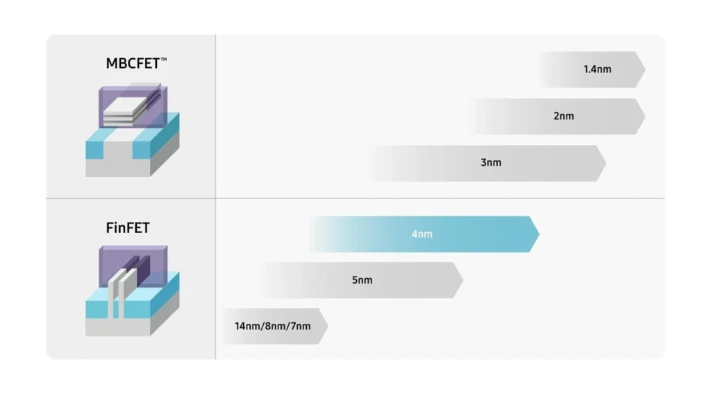
A report out of South Korea’s SEDaily says Samsung Foundry has crossed the 80% yield threshold on its 4nm FinFET process. That number matters. Yield rates at that level signal process maturity — the point where production stops being an expensive guessing game and starts being a reliable business.
Six years of mass production went into getting here. That’s not a typo. Samsung has been running 4nm at scale long enough that this milestone carries a different weight than it would for a newer node. The process is well understood at this point, the defects are mapped, and the fixes are baked in. What changes now is the economics.
Pyeongtaek Campus — which also handles 5nm and 7nm production — is positioned to feed 4nm chips to AI accelerator customers, the automotive sector, and mobile. That’s a wide spread of clients to be courting simultaneously. The more interesting application might actually be the base die for sixth-generation HBM4 memory chips, where the 4nm process sits underneath everything else in the stack.
TSMC isn’t losing sleep tonight, but Samsung doesn’t need it to. Demand for advanced chips from big tech is at levels where there’s room for more than one serious supplier, and Samsung is making a case that it belongs in that conversation again.
The company has had a rough stretch financially. Memory prices bit hard. A 4nm process that’s genuinely mature — not just marketable — gives Samsung something real to sell in the second half of this year when it needs the revenue to actually show up.